


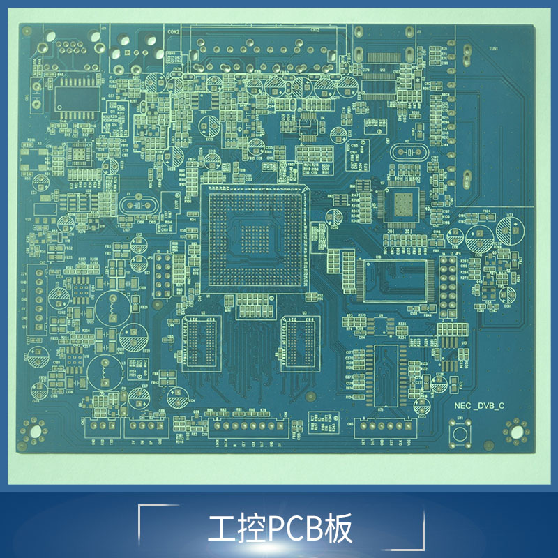
专业供应石岩四六层PCB线路板生产厂家 PCB线路板

专业供应石岩四六层PCB线路板生产厂家PCB线路板
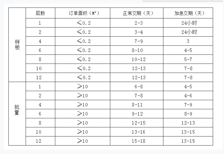
交期表
生产流程
1) Inner Layer 内层
> Chemical Clean 化学清洗
> Cut Sheet Dry Film Lamination 裁板 压膜
> Image Exp ose 曝光
> Image Develop 显影
> Copper Etch 蚀铜
> Strip Resist 去膜
> AOI Inspection AOI 检查
> Layup 叠板
> Vacuum Lamination Press 压合
2) CNC Drilling 钻孔
3) Outer Layer 外层
> Etch back - Desmear 除胶渣
> Electroless Copper 电镀-通孔
> Image Exp ose 曝光
> Image Develop 显影
4) Plating 电镀
> Copper Pattern Electro Plating 二次镀铜
> Tin Pattern Electro Plating 镀锡
> Strip Resist 去膜
> Copper Etch 蚀铜
> Strip Tin 剥锡
5) Solder Mask 阻焊
> LPI coating side 印刷
> Image Exp ose 曝光
> Image Develop 显影
6) Surface finish 表面处理
7) Profile 成型
8) ET Testing, continuity and isolation
9) QC Inspection > Pack & Shipping 包装及出货
(潍坊市PCB线路板厂家)
专业供应石岩四六层PCB线路板生产厂家 PCB线路板


线路板(pcb)
¥ 300.00
供应PCB线路板/PCB线路板供应电
面议
供应PCB线路板报价
面议
供应pcb线路板应
¥ 50.00
深圳PCB线路板制造商
¥ 28.00
供应龙华PCB线路板
面议
供应pcb线路板雕刻
面议
供应pcb线路板
面议
供应PCB刚性线路板
面议